Behaviour Box
An ESP32-S3 instrument for real-time stimulus delivery and data acquisition in neuroscience experiments.
Built with
- C
- ESP-IDF
- FreeRTOS
- SPI
- Eagle CAD
The problem with off-the-shelf I/O
Behavioral neuroscience experiments demand precise, repeatable timing: a tone plays, a valve opens, a reward is delivered. The animal’s response is recorded. Any jitter in that loop contaminates the data.
The usual answer is a commercial DAQ box — expensive, dependent on a driver stack, and not always available when the experiment lives on a cart in the animal room. The question was whether a small ESP32-S3 board, paired with a custom PCB, could hit the same timing targets for a fraction of the cost.
The answer is yes, with sub-millisecond response times measured end-to-end over USB.
Two cores doing different jobs
The ESP32-S3 has two cores, and keeping them focused on separate concerns is what makes the timing work.
Core 0 runs a tight FreeRTOS task that samples all digital inputs at 1 kHz and writes results into a mutex-protected ring buffer. It does nothing else. Any command that reads a digital input draws from that buffer — the answer is always fresh, never blocking.
Core 1 handles the USB Serial JTAG interface and processes incoming commands. When a command arrives, it either writes directly to a GPIO/SPI peripheral or reads from the buffer Core 0 is keeping warm.
Without this split, a slow analog read on Core 1 could delay the next buffer update on the same core, causing a missed sample. Separating them means the two timelines never interfere.
The protocol
Every message is exactly 7 bytes:
[0x33][PIN_TYPE][MODE][PIN][DATA_HIGH][DATA_LOW][0x0A]Fixed-length binary was a deliberate choice. There is no framing ambiguity, no text parsing, and the start/end bytes make it trivial to re-sync after a dropped byte. The host sends a command; the device responds with the same structure. Round-trip times measured over USB Serial JTAG at 1.5 Mbaud:
| Operation | Response time |
|---|---|
| Digital write | ~200 µs |
| Digital read | ~250 µs |
| ADC read | ~300 µs |
| DAC write (SPI) | ~400 µs |
The DAC path goes through an external AD5676 over an 8 MHz SPI bus — that leg is what pushes analog writes to 400 µs rather than the ~200 µs of a plain GPIO toggle.
Input buffering is not optional
The first version of the firmware had no background sampler. Reads were synchronous: command arrives, sample GPIO, respond. At low command rates that was fine. At rates above a few hundred Hz, samples were missed whenever the USB handler stalled.
The buffer loop on Core 0 fixes this structurally rather than by trying to make the USB path faster. A 1 ms sampling interval means that even if the command processor is busy for several milliseconds, no input transition goes undetected — the buffer captured it.
// Core 0 task — runs continuously, updates buffer at 1 kHz.
void input_buffer_task(void *arg) {
    TickType_t last_wake = xTaskGetTickCount();
    while (1) {
        xSemaphoreTake(buffer_mutex, portMAX_DELAY);
        for (int i = 0; i < NUM_INPUTS; i++) {
            bool level = gpio_get_level(input_pins[i]);
            if (level != input_buffer[i].state) {
                input_buffer[i].state   = level;
                input_buffer[i].changed = true;
            }
        }
        xSemaphoreGive(buffer_mutex);
        vTaskDelayUntil(&last_wake, pdMS_TO_TICKS(1));
    }
}
Hardware
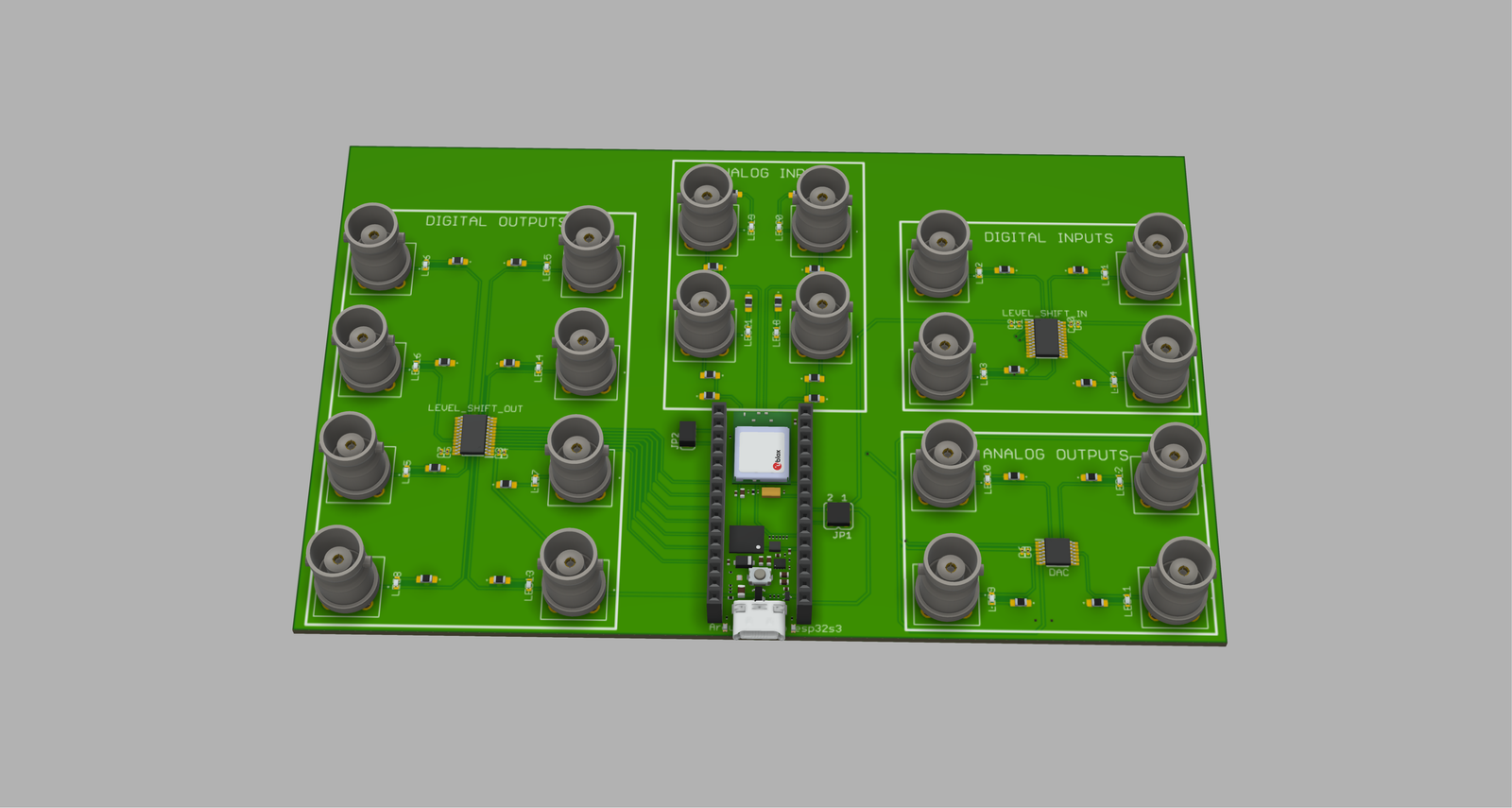
The PCB routes 8 digital outputs, 4 digital inputs, an SPI DAC header, and the ESP32-S3 module onto a board small enough to live in a standard instrument rack shelf. Gerber files, drill files, and a BOM are included in the repository — the board can be sent directly to a fab.
The design avoids any USB-to-serial converter chip. The ESP32-S3 has a hardware USB Serial JTAG peripheral that presents directly to the host OS as a CDC device, eliminating an entire class of latency and driver problems.